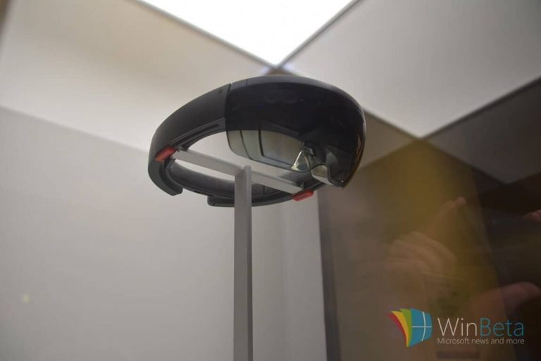
If you are the lucky owner of a HoloLens, you probably know a few things about the device. First on the list is its hefty price, and next up is probably the many uses and values developers have found. What you probably don’t know, however, is much about its internals, and the Holographic Processing Unit (HPU) which powers the device. Well, the secret is now out, and Microsoft has finally revealed more about the HPU of the Hololens (via The Register.)
The details on HPU on the Hololens were revealed today by Microsoft Devices Group engineer Nick Bakerat the Hot Chips conference in Cupertino, California. Overall, the HPU is a custom TSMC-fabricated 28nm coprocessor that has 24 Tensilica DSP cores. Additionally, with the coprocessor comes 65 million log gates, 8 MB of SRAM, and 1 GB of low-power DDR3 RAM. Lastly, an Intel Atom x86 Cherry Tail system on chip with 1 GB of RAM chip also powers the HPU on the device. In the words of The Register,
It handles all the environment sensing and other input and output necessary for the virtual-reality goggles. It aggregates data from sensors and processes the wearer’s gesture movements, all in hardware so it’s faster than the equivalent code running on a general purpose CPU. Each DSP core is given a particular task to focus on.
The HPU draws less than 10W and includes PCIe and standard serial interfaces. Overall, the unit is capable of accelerating algorithms to 200 times faster than when in pure software.
Data shuttled over to the host Atom processor is as cooked as possible, meaning the x86 CPU shouldn’t have to do lots of extra processing work on the information taken from the HPU.
So, there you have it! Those are the details on the HPU on the Hololens. What are your impressions? Did the specifications grab your attention? Let us know what you think by dropping us a comment below.